Example gates drawn in Magic
When the n-doped silicon (shown in green) crosses
polysilicon (shown in red), a nmos transistor is formed.
When the p-doped silicon (shown in brown) crosses
polysilicon (shown in red), a pmos transistor is formed.
When the control signal (on the polysilicon) is low (0):
- a pmos transistor is on, meaning it conducts electricity
- a nmos transistor is off, meaning it does not allow electricity
to flow
When the control signal (on the polysilicon) is high (1):
- a pmos transistor is off, meaning it does not allow electricity
to flow
- a nmos transistor is on, meaning it conducts electricity
So, a nmos or pmos transistor can be turned on to conduct electricity,
or turned off
so that it does not conduct electricity. Due to this property, we call
them semiconductors.
Together, the nmos and pmos form complimentary semiconductors. This is where we
get the term "cmos".
CMOS = Complimentary Metal-Oxide Semiconductor
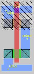
Inverter 
Blue represents metal, which allows electricity to flow. Think of the blue
paths as wires. The boxes (shown with a black X) are vias, and make a
connection between the different layers. For example, the two vias at the
bottom connect the layer shown in green (n-doped silicon) to the layer shown
in blue (metal).
When the input is high (1), the pmos transistor does not conduct, but the nmos
transistor does. Therefore, there is no path between the output and the supply
voltage (Vdd), but there is a path between the output and ground (GND). As
a result, the output would be low (0).
When the input is low (0), the pmos transistor conducts electricity, and
the nmos transistor does not. Therefore, there is a path between the output
and the supply
voltage (Vdd), but there is not a path between the output and ground (GND). As
a result, the output would be high (1).
This means that the output will always be the opposite of the input : and
we have an inverter.
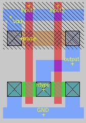
2 input NOR gate 
Notice how the pmos transistors are in serial,
while the nmos transistors are in parallel.
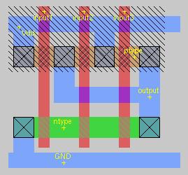
3 input NAND gate 
Notice how the pmos transistors are in parallel,
while the nmos transistors are in serial.
Since pmos is slower than nmos, a CMOS nand gate will be faster than a nor gate.
